Difference between revisions of "GEM1111"
Jump to navigation
Jump to search
| Line 81: | Line 81: | ||
| GND | | GND | ||
| 3,12 | | 3,12 | ||
| | | V<sub>SS</sub> | ||
| Ground | | Ground | ||
|- | |- | ||
| Line 99: | Line 99: | ||
| 2 | | 2 | ||
| O | | O | ||
| | | UART<sub>O</sub> serial data Tx. | ||
|- | |- | ||
| RXD<sub>0</sub> | | RXD<sub>0</sub> | ||
Revision as of 13:43, 11 May 2024
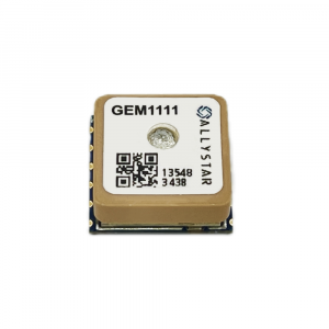
GEM1111 - 1616A00
1. Overview
GEM1111 is a high-performance L1 GNSS positioning module with antenna built-in, which is developed on the base of the state-of-the-art Allystar Cynosure III Lite architecture.
It supports global civil navigation systems, including GPS, BDS, GLONASS, Galileo, and QZSS. Featured with SAW and LNA, GEM1111 achieves high positioning accuracy and short TTFF,
especially in a rough urban environment.
It supports antenna supervisor and auto-switching between the built-in antenna and the external antenna.
With a compact body and high performance, GEM1111 is widely applied to tracking applications, like automotive, consumer, and industrial tracking.
Feature
- Supports GPS, BDS, Galileo, GLONASS, and QZSS systems Built-in LNA & SAW for better sensitivity
- Supports A-GNSS
- Supports geo-fence function
- Ultra-low power consumption around 13 mA in tracking mode
- Supports antenna supervision
- Supports auto-switching between the built-in antenna and the external antenna
1.1 Specifications
| Parameters | Specification |
|---|---|
| GNSS tracking channels | 72 channels, GPS/QZSS: L1C/A Galileo: E1 GLONASS: L1 |
| Updating rate | 1 Hz (Default), up to 5 Hz |
| Position accuracy | < 1.5 m CEP @ Open Sky |
| Velocity accuracy | 0.1 m/s CEP |
| Time accuracy | 1PPS 20ns |
| Time to First Fix(TTFF) | Hot start 1S Cold star 28S |
| Sensitivity | Cold start -149 dBm Reacquisition -159dBm Tracking -163dBm |
| Power supply | 2.0-3.63 V, Typical 3.3 V |
| Power consumption | Acquisition 15mA @3.3V Tracking 13mA @3.3V Standby mode 10uA |
| Serial Interface | UART Default: 115200 bps |
| Protocol | NMEA 0183 Protocol Ver.3.01/4.00 (Default)/4.10 |
| Operating temperature | -40~+85℃ |
| Storage temperature | -40~+85℃ |
| Weight | 7.5g |
| Dimessions | 16*16*6.9mm |
2.Pin description
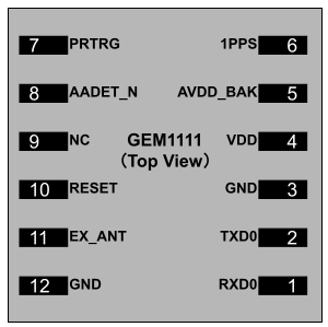
2.1 Pin assignment
2.2 Detailed pin description
| Function | Symbol | No | I/O | Decription |
|---|---|---|---|---|
| Power | VDD | 4 | Power | Main power supply voltage input. |
| GND | 3,12 | VSS | Ground | |
| AVDD_BAK | 5 | Power | Backup power supply voltage input. Backup power is needed in order to enable warm and hot start features. Backup power is a must for the system to work. If no backup power is available, connect AVDD_BAK to the main power supply. | |
| Antenna | RF_IN | 11 | I | RF signal input. Use a controlled impedance of 50 for the routing from RF_IN pin to the antenna or the antenna connector. |
| UART | TXD0 | 2 | O | UARTO serial data Tx. |
| RXD0 | 1 | I | UARTO serial data Rx. | |
| Other | PRTRG | 7 | I | Mode selection or the trigger input in deep sleep mode to wake up the system. |
| RESET | 10 | I | External reset, low active | |
| 1 PPS | 6 | O | Setting for time pulse output (PPS). Leave it floating if not used. | |
| AADET_N | 8 | O | Active antenna detection | |
| NC | 9 | Reserved. Leave it floating if not used. |
3.ELECTRICAL CHARACTERISTICS
3.1 Absolute Maximum Rating
| Symbol | Parameter | Min. | Max. | Unit |
|---|---|---|---|---|
| VDD | Power input for the main power domain | -0.5 | 3.6 | V |
| AVDD_BAK | Power input for the backup power domain | -0.5 | 3.6 | V |
| VImax | Digital I/O pin input voltage | -0.5 | 3.6 | V |
| Tstorage | Storage temperature | -40 | 85 | °C |
| Tsolder | Solder reflow temperature | -- | 260 | °C |
3.2 IO Characteristics
3.2.1 PRRSTX and PRTRG
| Symbol | Parameter | Condition | Min. | Typ. | Max. | Unit |
|---|---|---|---|---|---|---|
| IIZ | Input leakage current |
-- | -- | -- | +/-1 | uA |
| VIH | Input high voltage | -- | AVDD_BAK*0. 67 | -- | AVDD_BAK | V |
| VIL | Input low voltage | -- | 0 | -- | AVDD_BAK*0.27 | V |
| VOH | Output high voltage |
IOH=5.3 mA, AVDD_BAK=3.3V |
2.64 | -- | -- | V |
| IOH=1.2 mA, AVDD_BAK=1.8V |
1.53 | -- | -- | V | ||
| VOL | Output low voltage | IOL=3.9 mA, AVDD_BAK=3.3V |
-- | -- | 0.4 | V |
| IOL=1.9 mA, AVDD_BAK=1.8V |
-- | -- | 0.45 | V | ||
| Ci | Input capacitancee | -- | -- | -- | 11 | pF |
| RPU | Pull-up resistance | -- | 35 | -- | 84 | kΩ |
3.2.2 Others
| Symbol | Parameter | Condition | Min. | Typ. | Max. | Unit |
|---|---|---|---|---|---|---|
| IIZ | Input leakage current | -- | -- | -- | +/-1 | uA |
| VIH | Input high voltage | -- | VDD*0.67 | -- | VDD | V |
| VIL | Input low voltage | -- | 0 | -- | VDD*0.27 | V |
| VOH | Output high voltage | IOH =5.3 mA, VDD=3.3V | 2.64 | -- | -- | V |
| VOL | Output low voltage | IOL =3.9 mA, VDD=3.3V | -- | -- | 0.4 | V |
| Ci | Input capacitance | -- | -- | -- | 11 | pF |
Datasheet
Resource
ALLYSTAR_GNSS_Receiver_NMEA_Protocol_Specification
Common_Commands_Exclusive_to_Allystar

