TAU1312-datasheet
TAU1312 Multi-Band GNSS RTK Module
Feature
- Supports GPS, BDS, GLONASS, Galileo, and QZSS
- Compact size for high precision industry
- Integrated Real Time Kinematics (RTK)
- State-of-art low power consumption
- Supports multi-band multi-system high-precision raw data output, easy for 3rd party integration
- Highly integrated module, the best cost-effective high precision GNSS solution
- Compact size 12*16mm
Table 1 TAU1312 P/N
Product photo
Block diagram
Specifications
Table 2
| Parameter | Specifications | ||
|---|---|---|---|
| Constellations | BDS, GPS, QZSS, GLONASS, Galileo, NavIC, SBAS | ||
| Channel | 40 | ||
| Update rates | PVT 10Hz RTK 5Hz Max | ||
| Position accuracy | GNSS | 2.5m CEP | |
| SBAS | <1.0m CEP | ||
| RTK | 1.5 cm + 1 ppm (H) 6.5 cm + 1 ppm (V) | ||
| Velocity & Time accuracy | GNSS | 0.1 m/s CEP | |
| 1PPS | 20ns RMS | ||
| TTFF | Hot start | 2s | |
| Cold start | 24s | ||
| RTK | Convergence time | <10s | |
| Reliability | >99.9% | ||
| Sensitivity | Cold start | -148 dBm | |
| Hot start | -158 dBm | ||
| Reacquisition | -160 dBm | ||
| Tracking & navigation | -162 dBm | ||
| Protocol | NMEA-0183 V4.00/4.10 | ||
| RTCM 3.X | |||
| Baudrate | 115200 bps, by default | ||
| Operating condition | Main supply | 2.0V to 3.6V | |
| Digital I/O supply | 1.8V to 3.6V | ||
| Backup supply | 1.8V to 3.6V | ||
| Power consumption | Tracking | GNSS | 34 mA @ 3.3V |
| Single system | 22 mA @ 3.3V | ||
| Standby | Data backup | 12 uA | |
| RTC | 1.4 uA | ||
| Serial interface | UART | 1 | |
| SPI | 1 | ||
| I2C | 1 | ||
| Operating limit | Velocity | 515 m/s | |
| Altitude | 18,000m | ||
| Environmental conditions | Operating temp. | -40°C to +85°C | |
| Storage temp. | -40°C to +90°C | ||
| Humidity | 95% RH | ||
| Size | 16.0×12.2×2.4 mm, 24pin LCC | ||
GNSS Reception
Table 3 GNSS reception table
| P/N | OPTIONS | GPS/QZSS | BDS | GLONASS | GALILEO | IRNSS | |||||||||||
|---|---|---|---|---|---|---|---|---|---|---|---|---|---|---|---|---|---|
| L1C/A | L1C | L2C | L5 | L6 | B1I | B1C | B2I | B2a | B3I | L1 | L2 | E1 | E5 | E6 | L5 | ||
| TAU1312-1216A00 | A,L1+L5 | * | * | * | * | * | * | * | |||||||||
| B,L1+L2 | * | * | * | * | * | * | * | ||||||||||
PIN DESCRIPTION
Pin Assignment
Figure 3 Pin assignment (top view)
Detailed Pin Descriptions
Table 4 Detailed pin descriptions
ELECTRICAL CHARACTERISTICS
Absolute Maximum Rating
Table 5 Absolute rating
| Symbol | Parameter | Min. | Max. | Unit |
|---|---|---|---|---|
| VDD | Power input for the main power domain | -0.5 | 3.63 | V |
| AVDD_BAK | Power input for the backup power domain | -0.5 | 3.63 | V |
| AVDUSB | USB supply voltage | -0.5 | 3.6 | V |
| T storage | Storage temperature | -40 | 85 | °C |
| T solder | Solder reflow temperature | -- | 260 | °C |
IO Characteristics
PRRSTX and PRTRG
Table 6 PRRSTX and PRTRG
| Symbol | Parameter | Condition | Min. | Typ. | Max. | Unit |
|---|---|---|---|---|---|---|
| I IZ | Input leakage current | -- | -- | -- | +/-1 | uA |
| V IH | Input high voltage | -- | AVDD_BAK*0. 7 | -- | AVDD_BAK | V |
| V IL | Input low voltage | -- | 0 | -- | AVDD_BAK*0.3 | V |
| C i | Input capacitance | -- | -- | -- | 10 | pF |
| R PU | Pull-up resistance | -- | 18 | -- | 84 | kOhm |
USB I/O
Table 7 USB signal
Others
Table 8 Others
DC Characteristics
Operating Conditions
Table 9 Operating Conditions
Power Consumption
Table 10 Power consumption
HARDWARE DESCRIPTION
Connecting Power
Power on/off Sequence
Initial system power on
Main power supply off/on in application
Antenna design
Reset and mode control
Default Serial interfaces
Table 11 Default message
| Interface | Settings |
|---|---|
| UART output | 115200 baud, 8 data bits, no parity bit, 1 stop bitConfigured to transmit both NMEA and HD Binary protocols, but only the following NMEA (and no HD Binary sentence) messages have been activated at start-up: GGA, GSA, GSV, RMC, ZDA, TXT-ANT |
| UART input | 115200 baud, 8 data bits, no parity bit, 1 stop bit, autobauding disabled Automatically accepts following protocols without need of explicit configuration: HD binary sentence, NMEA, RTCM The GNSS receiver supports interleaved HD binary and NMEA messages. |
| Timepulse,(1Hz Nav) | 1 pulse per second, synchronized at rising edge, pulse length 100ms |
5 MECHANICAL SPECIFICATION
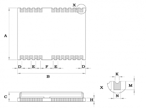
Figure 6 Dimensions
Table 12 Dimensions
| Symbol | Min.(mm) | Typ.(mm) | Max.(mm) |
|---|---|---|---|
| A | 12.0 | 12.2 | 12.4 |
| B | 15.8 | 16.0 | 16.2 |
| C | 2.2 | 2.4 | 2.6 |
| D | 0.9 | 1.0 | 1.3 |
| E | 1.0 | 1.1 | 1.2 |
| F | 2.9 | 3.0 | 3.1 |
| H | -- | 0.8 | -- |
| K | 0.4 | 0.5 | 0.6 |
| M | 0.8 | 0.9 | 1.0 |
| N | 0.7 | 0.8 | 0.9 |
REFERENCE DESIGN
Minimal design
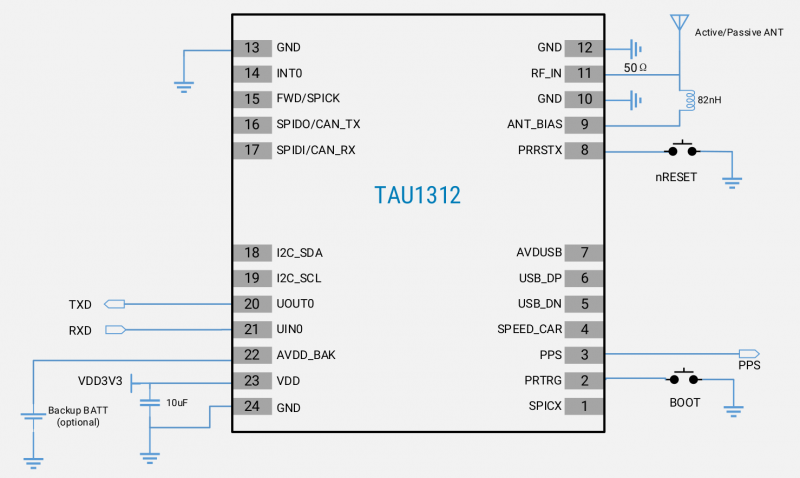
This is a minimal design for TAU1312 GNSS module. The 82nH inductor is used only when an active antenna is connected, and no need with a passive antenna. The characteristic impedance from RF_IN pin to the antenna connector should be 50Ω.
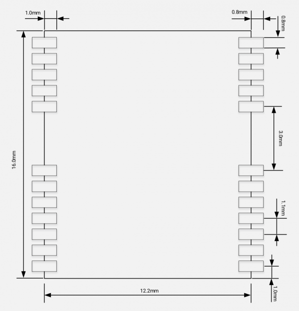
PCB Footprint Reference
Layout
(1) A decoupling capacitor should be placed close to VDD pin of the module, and the width of power routing should be more than 0.5mm.
(2) The width of RF routing between RF port to antenna interface should be wider than 0.2mm. The characteristic impedance of RF routing between RF port to antenna interface should be controlled to 50Ω.
(3) It is recommended that the routing from RF port to antenna interface refers to the second layer,and no routing are recommended on the layer.
(4) Do not place the module close to any EMI source, like antenna, RF routing, DC/DC or power conductor, clock signal or other high-frequency switching signal, etc.
PRODUCT PACKANG AND HANDLING
Packaging
Packing Notes
Tape and Reel
Shipment Packaging
Storage
ESD Handling Precautions
ESD protection measures
Moisture sensitivity level
The Moisture Sensitivity Level (MSL) of the GNSS module is MSL4.
LABELING AND ORDERING INFORMATION
Labeling
Ordering info
Table 15 P/N


